
“Design-for-Testability (DFT) is a critical element in the design of modern, high-performance digital systems.” – Jacob A. Abramovici, electrical engineer and computer scientist, and author of the book Digital Systems Testing and Testable Design.
Design for testability is not just a nice-to-have feature anymore. It is essential for ensuring that chips can be tested efficiently and effectively, without compromising on quality or reliability – Dr. V.Nithish Kumar, Associate Professor Grade I, Vellore Institute of Technology, Vellore.
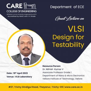
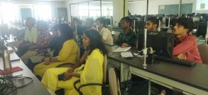
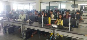
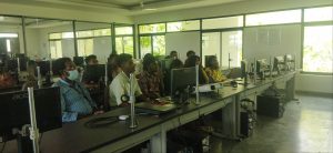
Department of Electronics and Communication Engineering organized a guest lecture “VLSI – Design for Testability” on 19th April, 2023. The guest lecture was given by a well-known expert in the field Dr.V.Nithishkumar, Associate Professor Grade I, Vellore Institute of Technology, Vellore. The lecture covered various topics related to designing chips for easy testing, including Design for Test (DFT), Scan chains, Built-In Self-Test (BIST), and other related techniques.
The lecture started with an introduction to the importance of testing in the chip design process. The speaker emphasized that testing is critical to ensure that chips function correctly and meet their specifications. However, testing can also be expensive and time-consuming, which is why design for testability (DFT) is becoming increasingly important.
The speaker then discussed various DFT techniques, starting with scan chains. Scan chains are a way of connecting the flip-flops in a chip to a test controller, allowing for easy testing of the chip’s functionality. The speaker explained how scan chains work and why they are so useful for testing. Next, the speaker discussed Built-In Self-Test (BIST), which is another popular DFT technique. BIST involves building a test controller into the chip itself, which allows for testing without the need for external test equipment. The speaker explained the advantages and disadvantages of BIST and gave examples of how it can be used.
The lecture then moved on to other DFT techniques, such as boundary scan and memory BIST. The speaker explained how these techniques work and how they can be used to improve the testability of chips.
Towards the end of the lecture, the speaker discussed some of the challenges associated with DFT. One of the main challenges is balancing the tradeoff between test coverage and test time. The more comprehensive the testing, the longer it takes to complete. The speaker also discussed how DFT can impact chip design, and how designers need to consider testability early in the design process.
Overall, the lecture provided an excellent overview of VLSI design for testability. The speaker did an excellent job of explaining complex concepts in an accessible way, and the lecture was well-structured and easy to follow. The students learned a lot about different DFT techniques and the challenges associated with designing chips for testability.
The lecture was coordinated by Mr. Sriram Sundar S, Assistant Professor I, CARE College of Engineering.